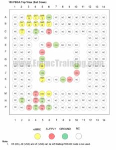
BGA 153 Isp Pinout | Bga 153 Test Point
Each BGA chip is identified by the number of PIN it contains a BGA 153 would have place on 153 PIN’s on PCB surface. In addition, a BGA can have different form factor variants. SMD ball grid array, BGA packages enable high density connections to be made more easily to integrated circuits by allowing the under-side of a chip package to be used for the connectivity.The Ball Grid Array has become increasingly popular for SMD ICs that require high density connections. Using the under-side of the IC package rather than connections around the edge, this enables connection density of be reduced, simplifying PCB layout.
BGA 153 Pin Configuration

Here is Our Video Tutorial :
What is ISP Pinout ?
ISP means “In-System Programming”.In-System Programming (ISP) allows communication to take place with a target chip without the need to remove it. The main advantage of this method is the possibility to communicate with a target chip eMMC or eMCP bypassing the CPU. It brings higher speed for data extraction compared with JTAG but it requires great soldering skills. ISP applied to forensics, is the practice of connecting to an eMMC or eMCP flash memory chip for the purpose of downloading a device’s complete memory contents.
eMMC and eMCP memory are the standard in today’s smartphones, and the ISP practice enables examiners to directly recover the complete data without removing the chip and destroying the device.ISP benefits the examiner who faces the challenges of tightening budgets, yet wants to expand their expertise in retrieving evidence from locked smartphones. A cost-effective technique, ISP provides examiners with the same results of a chip-off at a lower price-point.
Why do we need ISP Pinout ?
Just Like “Joint Test Action Group (JTAG)” there are specific contacts that will be of interest to the examiner. But unlike JTAG, the contacts are directly off the chip BGAs and do not go through the processor. Acquires data much faster than JTAG, enabling examiners to process more phones faster.
- CMD
- CLK
- DATA0
- GND
- VCC – Voltage Supply for Core (3,3V)
- VCCQ – Voltage Supply for I/O (1,8 – 3,3V)
The purpose of each signal is as follows:-
CLK : Clock signal for synchronization.Each cycle of this signal directs a one bit transfer on the command and either a one bit (1x) or a two bits transfer (2x) on all the data lines. The frequency may vary between zero and the maximum clock frequency
CMD : This signal is used to send the Host’s command and Device’s response.
Data0 : These are bidirectional data channels. The DAT signals operate in push-pull mode. Only the Device or the host is driving these signals at a time. By default, after power up or reset, only DAT0 is used for data transfer. A wider data bus can be configured for data transfer, using either DAT0-DAT3 or DAT0-DAT7, by the eMMC host controller. The eMMC Device includes internal pull-ups for data lines DAT1-DAT7. Immediately after entering the 4-bit mode, the Device disconnects the internal pull ups of lines DAT1, DAT2, and DAT3. Correspondingly, immediately after entering to the 8-bit mode the Device disconnects the internal pull-ups of lines DAT1–DAT7.
GND : VSS is the Ground for Core & VSSQ is the Ground for I/O.
VCC : VCC is the Power Supply for Core.
VCCQ : VCCQ is the Power Ssupply for I/O.
