What is BGA (Ball Grid Array)
BGA components are packaged electronically into standardized packages that include a wide array of shapes and sizes. It is well-known for its minimal inductance, high lead count and remarkably effective density. Ball grid array (BGA) is a type of surface mount technology (SMT) that is used for packaging integrated circuits. BGA is made up of many overlapping layers that can contain one to a million multiplexers, logic gates, flip-flops or other circuits.
SMD ball grid array, BGA packages enable high density connections to be made more easily to integrated circuits by allowing the under-side of a chip package to be used for the connectivity.The Ball Grid Array has become increasingly popular for SMD ICs that require high density connections. Using the under-side of the IC package rather than connections around the edge, this enables connection density of be reduced, simplifying PCB layout.
The main problem with using SMD BGA IC packages is that using the under-side of the chip means that direct access to the connections is not possible, making soldering, de-soldering and inspection more difficult. However with mainline PCB production equipment, these issues are easy to overcome and the overall reliability and performance can be improved.
Ball grid array (BGA) is a common surface mount package derived from pin grid array (PGA) technology. It uses a grid of solder balls or leads to conduct electrical signals from the integrated circuit board. Instead of pins like the PGA, the BGA uses solder balls that are placed on the printed circuit board (PCB). By using conductive printed wires, the PCB supports and connects electronic components.
Unlike the PGA, which has hundreds of pins that makes soldering difficult, BGA solder balls can be spaced evenly apart without accidentally bridging them together. The solder balls are first placed on the bottom of the package in a grid pattern and then heated. By using surface tension when melting the solder balls, the package can be aligned with the circuit board. The solder balls cool and solidify with an accurate and consistent distance between them.
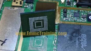
BGA Example :
BGA is made of conducting and insulating layers with a solder mask that is normally green in color but can be black, blue, red or white. The conducting layers are usually composed of thin copper foil that can be specified in micrometers or ounces per square foot. The insulating layers are generally bonded together with epoxy resin composite fibers “pre-preg”. The insulation material is dielectric.
Each BGA chip is identified by the number of PIN it contains a BGA 153 would have place on 153 PIN’s on PCB surface. In addition, a BGA can have different form factor variants.
Here Is Our Tutorial Video :